Electron emission modelling for ultra-high voltage holding and electron sources
Contact: Tiberiu Minea
This area of research at LPGP focuses on understanding electronic emission from micro/nano-structures on the surface of a high-voltage vacuum cathode [1].
Our model describes field-effect induced emission (AC or DC) with a thermionic contribution and in some cases includes photoelectric emission. The modelling work has two applications in view: the involvement of electronic emission from surface asperities in the vacuum breakdown of ultra-high-voltage devices, and the study of field-effect electron sources based on micro/nano-emitter assemblies.
The most significant results have been brought together in a book [1] that introduces the physics and the main phenomena that govern electronic emission at high fields and temperatures. It presents recent approaches to numerical modelling and advanced developments, and is an important resource for Masters and PhD students wishing to study field emission, the behaviour of high-voltage devices, laser irradiation of surfaces and vacuum breakdown, as well as for researchers and industrialists in the field of accelerators and solid-state physics with an interest in these phenomena.
High voltage withstand under vacuum
The first emission model was developed to evaluate the electronic emission from a single micro-structure. This model was first extended to an axially symmetric 2D geometry with time dependence and taking into account the self-heating of the micro-structure during emission. The results obtained in collaboration with the GeePS laboratory (CentraleSupelec) demonstrated that by applying a pulsed field (ns), it was possible not only to extract more electrons from the cathode, but also to increase the voltage withstand before breakdown. The shielding induced by the space charge during thermo-emission assisted by intense electric fields has been studied and, while maintaining the same maximum current emitted, it has been shown that voltage withstand is better when the space charge is present [2].
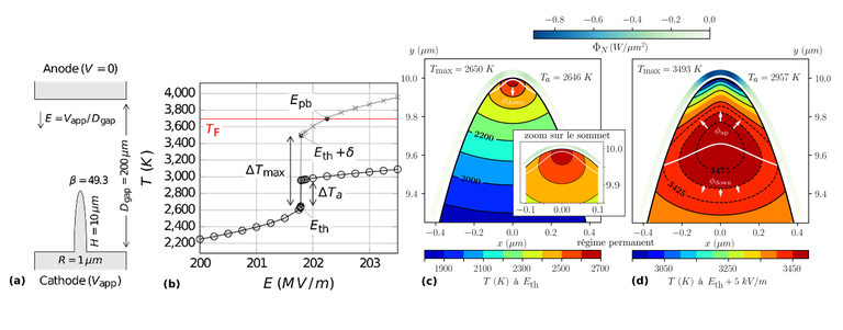
The continuation of this work (thesis by D. Mofakhami [3], 2018-2021) has made it possible - by refining the temporal evolution of the self-heating of the emitters - to differentiate between the stable evolution towards a steady state and the development, under certain conditions, of a thermal instability caused by the positive feedback loop between resistive heating and emitted current. In addition, a certain range of parameters has been identified for which the competition between resistive heating and the Nottingham effect, which becomes cooler (at high temperature), leads to the observation of a bi-stability around a threshold field. This bi-stability is associated with a jump in temperature, as shown in Figure 1.)
Field effect electron sources based on emitter arrays
In addition, the extension of the model to 3D geometry has opened the way to the study of real, or at least realistic, field emitter arrays (FEAs). These more or less regular arrangements are at the heart of a new field-effect electron source technology that could eventually achieve intensities equivalent to their thermionic counterparts, without the disadvantages.
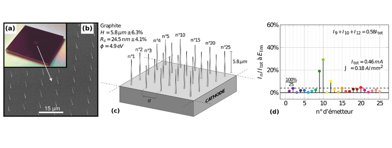
Working from independent experimental measurements, our simulations have recently made it possible to estimate the influence of the growth statistic of an emitter array on its emission performance (see [3], Chapter 6). Figure 2 shows, for example, for a given statistical distribution, the relative contribution of each emitter in an array to the total current. Combined with a thermal destruction model, this type of simulation could eventually become a good tool for assessing the effects of network parameters on source robustness and lifetime.

FIGURE 1 – Observation of bi-stability around the Eth threshold field for a single tungsten hemi-ellipsoid emitter. (a): Schematic diagram of the modelled configuration. (b) : Variation of the maximum temperature Tmax with the applied field E and of the temperature at the top Ta in steady state. δ=5kV/m, so that δ/Eth=0.002%. (c): Steady-state temperature distribution at Eth and (d):at Eth+δ. Parameter ΦN gives the heat flux density removed by the Nottingham effect at the emission surface.

FIGURE 2–Influence of the growth statistic on the relative contribution of the emitters to the total current of a regular array of carbon nanocones. (a): 1cm×1cm chip engraved on 1mm×1mm. (b) : SEM micrograph of the carbon nanocones on the etched surface (c) : Diagram of the simulated situation (25 emitters from a Gaussian draw on the height H and the radius at the apex Rs). (d): Contribution to total current Itot of each of the 25 transmitters at the field limit Elim just before the thermal destruction of emitter no. 10. J is the corresponding macroscopic current density.
Bibliography
[3] Darius MOFAKHAMI. “Modélisation Multiphysique de l’émission Électronique Par Effet de Champ d’une Surface 3D Micro/Nano-Structurée”. Ph. D Thesis of Paris-Saclay university, march 2022.
