Ultra-thin films and nanoparticles using magnetron plasma
Contact : Pierre BILLAUD
1) Ultra-thin films
Thin and ultra-thin films (< 100 nm) have many applications in optics, electronics, electrical engineering, photonics, spintronics, aerospace, healthcare, fuel cells and more. One highly effective method of producing these films is sputtering, a process in the PVD (Physical Vapour Deposition) family. The magnetron sputtering process is the most widely used. Plasma can be created in direct current (DCMS - Direct Current Magnetron Sputtering), radio frequency (RF), high-power pulse mode (HiPIMS - High Power Impulse Magnetron Sputtering) or hyper-power mode (HyPIM - Hyper Power Impulse Magnetron). We also have arc-type systems (under vacuum or close to atmospheric pressure). The laboratory has a clean room and several (multi-target) magnetron reactors enabling the growth of various single-element films (metal, carbon, silicon, etc.), stacks of several nano-layers, or compounds (oxides, nitrides, oxi-nitrides, etc.) [REF 1,2].
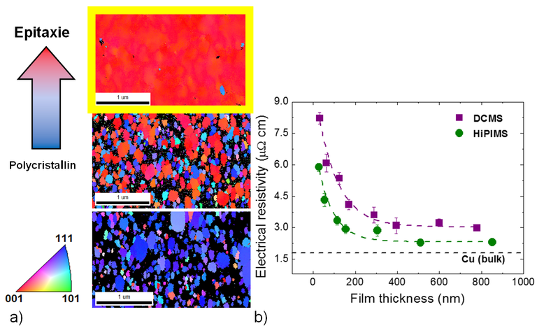
By way of example, epitaxial copper (Cu) layers have been produced by HiPIMS magnetron (Figure a - [REF 3]). The electrical conductivity of these layers is close to that obtained by filtered arc and very close to that of the bulk for thicknesses well below 100 nm (Figure b - [REF 4]). It should be noted that the process used is easily accessible and that these films were obtained without any pre-treatment of the substrate.

a) Growth of an ultra-thin (< 100 nm) Cu epitaxial layer [REF 3].
b) comparison of electrical resistivity as a function of deposit thickness between the conventional process (DCMS) and HiPIMS [REF 4]. For a 100 nm film, the resistivity is only 2 times that of the bulk.
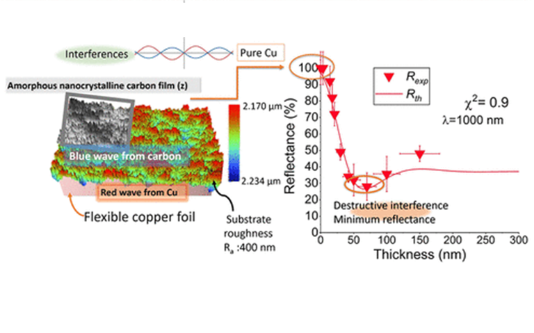
In a second example, the multi-layer interferometric effect is demonstrated in the case of reducing the reflectance of a super-reflective surface (in this case Cu). It is shown that the conformal growth of an ultra-thin film (< 100 nm, here made of C of the DLC - Diamond Like Carbon - type) is possible on substrates with high roughness (> 2 µm). In addition, this type of semi-metallic, semi-transparent film absorbs some of the radiation, but also allows some to pass through and be reflected off the substrate (Cu). The wave thus reflected passes through the film a second time and can arrive in phase opposition. Using electromagnetic modelling at several interfaces, it is therefore possible to explain the phenomenon observed experimentally, highlighting an optimum thickness (between 25 and 60 nm, depending on the wavelength). Absorption @ 1 µm falls from 99% to around 30% (Figure 2, [REF 5]). Increasing the layer thickness beyond 50 nm does not improve the result and would require a longer deposition time. It should also be noted that the process can easily be scaled up, as is the case with all PVD coatings.
These films enable better management of energy transfer and can make an effective contribution to combating global warming.

Figure 2 : Example of destructive interference using a carbon layer of around 50 nm on a copper surface with a roughness of several µm. Conformal deposition was achieved by DCMS magnetron. [REF 5]
2) Nanoparticles
A new aspect of this activity aims to use PVD to produce aggregates of a few atoms to a few dozen atoms, or even nanoparticles. The fundamental aspect aims to gain a better understanding of the phenomena of coalescence in the gas phase and the possibility of having a process that is selective according to the size of the nanoparticles. The deposition of aggregates (e.g. ILM collaboration) on ad hoc substrates (e.g. L2C collaboration) can lead to the formation of nano-objects with branched shapes. These multi-scale dendritic nanostructures (qq. nm to qq. 100 nm) with a non-integer fractal dimension (e.g. LAC collaboration) are called nanofractals (paper in preparation). Optical characterisation in the laboratory of substrates coated with nano-structures will be used to broaden the field of study of their properties.
In terms of applications, this magnetron process will be offered as an alternative to thermal evaporation or laser vaporisation, the productivity and scale-up of which are still questionable.
[REF 1] F Cemin, M Tsukamoto, J Keraudy, V Antunes, UHelmersson, F Alvarez, T Minea, and D Lundin,
Low-energy ion irradiation in HiPIMS to enable anatase TiO2 selective growth
2018 J. Phys. D: Appl. Phys. 51 (2018) 235301; doi: 10.1088/1361-6463/aac080
[REF 2] F. Cemin, G. Abadias, T. Minea, D. Lundin
Tuning HiPIMS discharge and substrate bias conditions to reduce the intrinsic stress of TiN thin films
2019 Thin Solid Films 688 (2019) 137335-https://doi.org/10.1016/j.tsf.2019.05.054
[REF 3] F.Cemin, D. Lundin, C.Furgeaud, A. Michel, G.Amiard, T. Minea, and G. Abadias
Epitaxial growth of Cu(001) thin films onto Si(001) using a singlestepHiPIMS process
2017 Scientific Reports 7, 1655 ; doi:10.1038/s41598-017-01755-8
[REF 4] F. Cemin, D. Lundin, D. Cammilleri, T. Maroutian, P. Lecoeur, T. Minea
Low electrical resistivity in thin and ultrathin copper layers grown by high power impulse magnetron sputtering
2016 J. Vac. Sci Technol. A 34, 051506; doi: 10.1116/1.4959555
[REF 5] A. Crespi, Ch. Ballage, M-C Hugon, D. Lundin, T. Minea
The role of amorphous nanocrystalline carbon film in the light interference of flexible copper foils
ACS Appl. Electron. Mater., 4, (2)(2022) 576–584, https://doi.org/10.1021/acsaelm.1c00520
